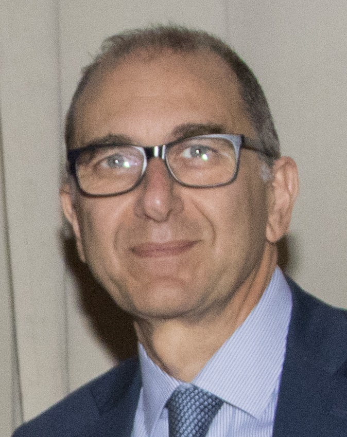
Antonio Terrasi
Ruolo: Consigliere d’Amministrazione
Indirizzo mail: antonio.terrasi@ct.infn.it
Nota Biografica
ANTONIO TERRASI
Education and roles
Graduation in Physics with honors in 1986 at the University of Catania.
PhD in Physics in 1990.
Visiting Scientist at the Synchrotron Radiation Center of the University of Wisconsin-Madison (U.S.A.) for various periods in the years 1988, 1989 and 1990. In particular from September 1988 to June 1989 continuously in the context of the PhD.
Scientific Officer at the École Polytechnique Fédérale de Lausanne (E.P.F.L.) throughout 1994.
Researcher at the National Research Council 01-01-1995 to 30-03-1997.
Researcher at the University of Catania 01-04-1997 to 19-03-2005.
Associate Professor of Experimental Physics at the University of Catania 20-03-2005 to 30-09-2018
Oridnario Professor of Experimental Physics at the University of Catania since 1-10-2018.
Coordinator of the PhD in “Materials Science” of the University of Catania XVIII to the XXI cycle.
Vice-coordinator of the PhD in “Materials Science and Nanotechnologies” up to the XXXI cycle.
Currently member of the Teaching Board of the PhD in “Materials Science and Nanotechnologies” of the University of Catania.
Member of the Quality Department of the Physics and Astronomy Department.
Referent of the University of Catania for the framework agreement with the Colorado School of Mines (USA) for the five-year period 2014-2018.
Referent of the University of Catania for the “Blue Italian Growth” National Technology Cluster since October 2016
Referent of the University of Catania for the permanent strategic technical table in the ENERGY field at the Regional Department of Productive Activities since June 2017.
Referent of the University of Catania of the framework agreement between the University and ENEL since October 2017.
Referent of the University of Catania of the framework agreement between the University and ENEA.
Academic Senator of the University of Catania November 2106 to Oct. 2018.
Rector’s Delegate for Technology Transfer and relationships with enterprises.
Research activity fields
Absorption (EXAFS) and photoemission (XPS) spectroscopies with synchrotron radiation and laboratory X-ray sources;
Electronic and structural analysis of semiconductor and insulating materials through electrical measurements, optical and electronic microscopies, Rutherford backscattering of light ions (RBS);
Use of low energy ion beams for assisted processes of film modification and oxidation of surfaces;
Thin film growth by evaporation in ultra high vacuum systems.
Formation of clusters for ion implantation, low energy ion bombardment and ultra high vacuum evaporation;
Studies of the electronic structure of metal / semiconductor interfaces and heterojunctions (photoelectronic spectroscopies);
Electronic structure of high critical temperature superconductors (photoelectronic spectroscopies);
Electronic structure of low-dimensional compounds and study of Charge Density Waves transitions (photoelectronic spectroscopies);
Formation of silicides and deposition of thin films on silicon with ion beam assisted evaporation processes (CoSi2, -FeSi2, Al / Si) (electron microscopy, photoemission spectroscopy, RBS);
Formation of ultra-thin SiO2 films through high temperature thermal processes or processes at room temperature assisted by ion beams (electrical measurements, electron microscopies, photoelectronic spectroscopies);
Growth of Si doped with Er and O for ion implantation and for MBE epitaxial deposition (electrical measurements, optical measurements, microscopies, EXFAS spectroscopy, RBS);
Epitaxial growth MBE of doped Si with B for diffusion studies;
MBE epitaxial growth of Si, Si (1-x) Ge (x) and Si (1-x) C (x) alloys (structural and electrical measurements) and of Ge and SiGe nanostructures;
Synthesis and structural-electrical-optical characterization of Si and Ge nanocrystals in oxide, nitride and Si carbide for applications in photodetectors and third generation photovoltaic cells.
Synthesis and characterization of Ge nanocrystals by colloidal way for applications in photodetectors.
Synthesis and characterization of thin films of Conductive Transparent Oxides (TCO) and Conductive Transparent Materials (TCM) based on TCO / Ag / TCO nanometric multilayers, also with Ag nanogrids, for photovoltaic applications.

